HOME
ABOUT US
Company Profile
Workshop
Service
FAQ
APPLICATIONS
Electronics & Semiconductor
Optical & Filtration Applications
Automotive & Industrial
Medical & Consumer Electronics
Cultural & Custom Gifts
COMPONENTS
Stainless Steel
Brass
Aluminum
Nickel & Nickel Alloys
Iron & Alloy Steels
Precious & Specialty Metals
BLOG
Advantages
Tolerances of etchining
Workflow of Chemical Etching
CONTACT US
Home
APPLICATIONS
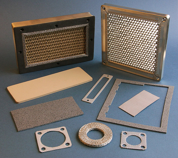
EMI/RFI Shielding Covers
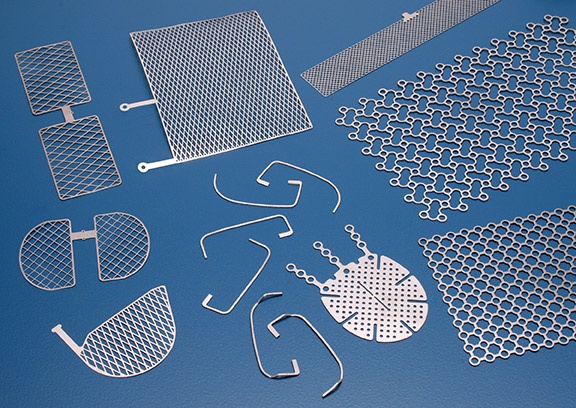
Precision Electrodes & Contact Sheets
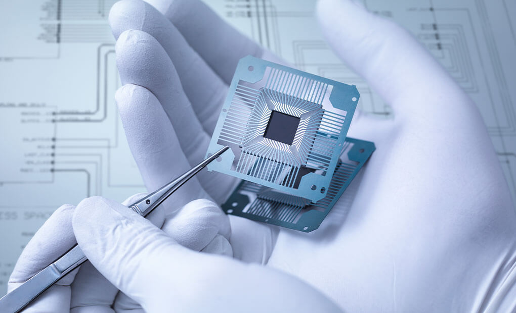
Semiconductor Lead Frames
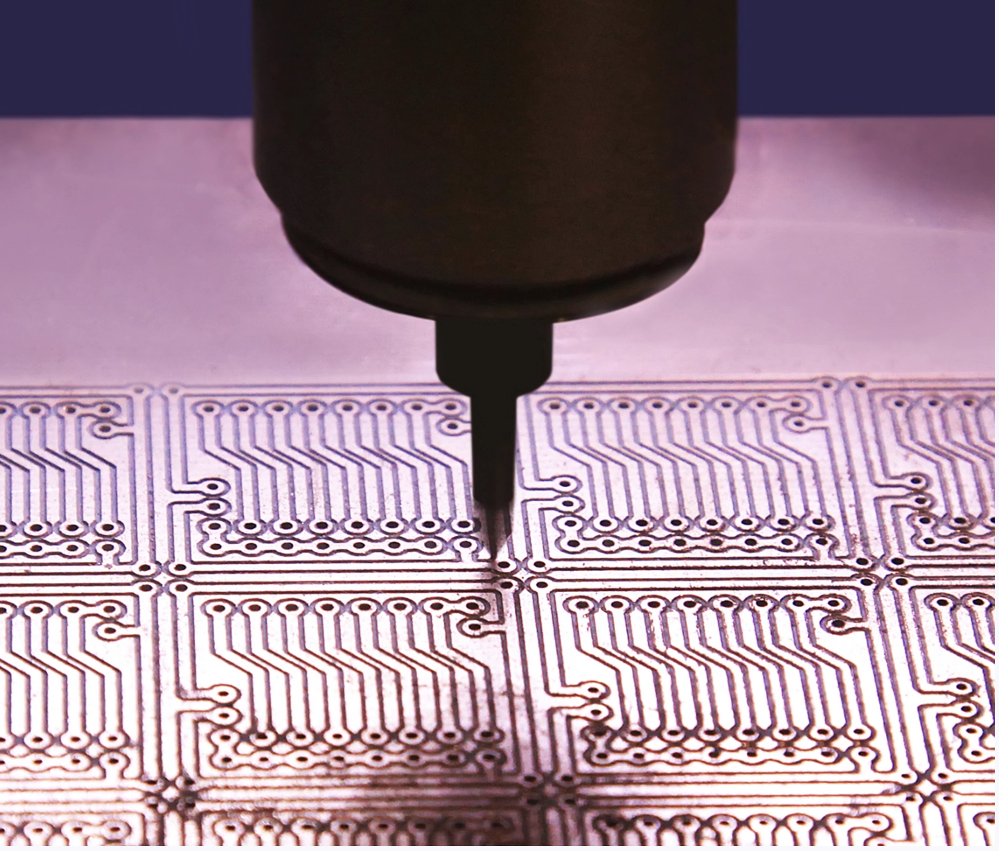
PCB Inner Metal Layers
Chemical Etching in Medical & Consumer Electronics Applications
Advanced Metal Etching for the Automotive Industry
The Application of Chemical Etching in Automotive and Industrial Sectors
The Application of Chemical Etching in Optical and Filtration Industries
The Role of Chemical Etching in Cultural and Custom Gifts
1
Get the latest price? We'll respond as soon as possible(within 12 hours)
Name
Size
Operate
Upload
Please submit your drawings to us. Files can be compressed into ZIP or RAR folder if they are too large.
We can work with files in format like pdf, sat, dwg, rar, zip, dxf, xt, igs, stp, step, iges, bmp, png, jpg, doc, xls, sldprt.
Submit
HOME
ABOUT US
Company Profile
Workshop
Service
FAQ
APPLICATIONS
Electronics & Semiconductor
Optical & Filtration Applications
Automotive & Industrial
Medical & Consumer Electronics
Cultural & Custom Gifts
COMPONENTS
Stainless Steel
Brass
Aluminum
Nickel & Nickel Alloys
Iron & Alloy Steels
Precious & Specialty Metals
BLOG
Advantages
Tolerances of etchining
Workflow of Chemical Etching
CONTACT US
العربية
Deutsch
English
Español
Français
हिन्दी
한국어
Português
Svenska
Türk