
Chemical Etching Technology for Precision Electrodes and Contact Sheets
In high-performance electronic and electrical systems, precision electrodes and contact sheets play a critical role in ensuring stable conductivity, accurate signal transmission, and long-term durability. These components are widely used in batteries, sensors, medical instruments, automotive connectors, and communication devices — all of which demand exceptional dimensional precision and surface integrity.
Traditional manufacturing techniques such as stamping, wire cutting, or laser machining often struggle to achieve the fine geometries, stress-free edges, and material consistency required for today’s miniaturized designs. To meet these challenges, manufacturers increasingly rely on chemical etching technology, also known as photochemical machining (PCM) — a process that combines photolithography and controlled chemical dissolution to create ultra-precise metal parts without mechanical stress.
1. The Role of Precision Electrodes and Contact Sheets
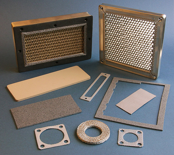
Electrodes and contact sheets serve as conductive interfaces that enable electrical current to flow efficiently between components. In applications such as lithium-ion batteries, fuel cells, and sensors, electrodes must feature high conductivity, corrosion resistance, and precise microstructures that control current density and chemical reactions.
In connectors and switching systems, contact sheets must maintain tight tolerances for both dimensional accuracy and surface finish to ensure consistent contact resistance and mechanical fit. As devices become smaller and more compact, the need for ultra-thin, high-density electrode patterns has made traditional fabrication methods increasingly inadequate.
Chemical etching provides a solution that combines micron-level precision, design flexibility, and excellent material preservation, making it ideal for producing the next generation of precision electrodes and contacts.
2. The Photochemical Etching Process
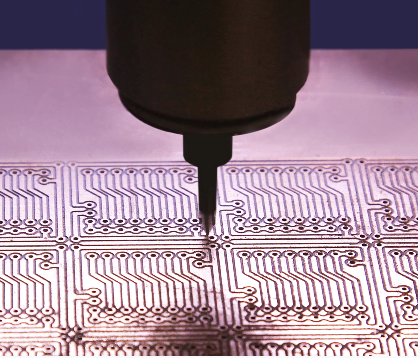
The process begins with a thin sheet of conductive metal such as copper, stainless steel, nickel, titanium, or molybdenum, depending on the application. The surface is first cleaned and laminated with a photoresist — a light-sensitive film. The desired pattern is then transferred onto the sheet using UV exposure through a digital photomask.
After development, the exposed metal areas are selectively dissolved in a chemical etchant, such as ferric chloride or cupric chloride. This controlled corrosion removes material only where required, leaving behind perfectly defined electrodes or contact geometries. The remaining photoresist is then stripped, and the clean, burr-free metal structure is revealed.
Because this process is contact-free and stress-free, it does not deform, crack, or harden the material. The resulting components exhibit smooth edges, uniform thickness, and precise detail — critical attributes for electrical performance and assembly accuracy.
3. Superior Precision and Design Flexibility
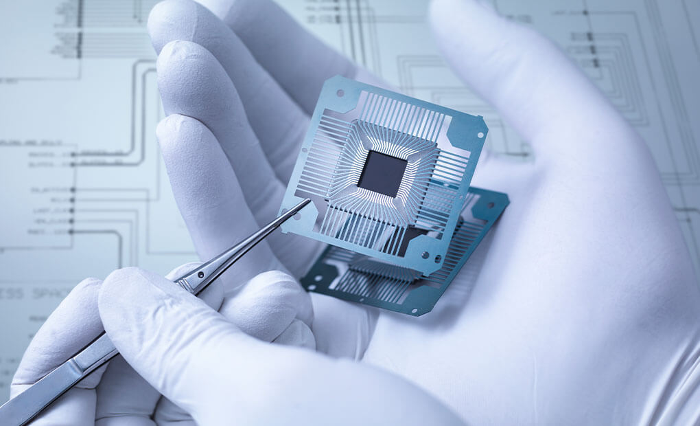
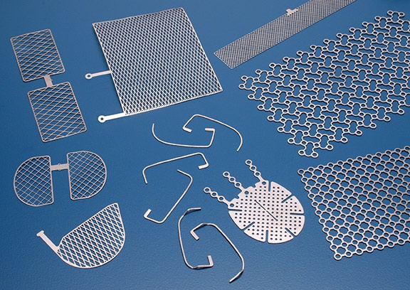
Chemical etching allows for the creation of complex and extremely fine patterns that are difficult or impossible to produce by mechanical methods. Line widths and gaps as small as 50 μm can be achieved with consistent repeatability. This capability makes the process ideal for microelectrodes, fine-pitch contact grids, microcurrent collectors, and sensor arrays.
In addition, since tooling is digital rather than mechanical, design modifications can be implemented quickly and cost-effectively. Prototypes can be produced in a matter of days without expensive molds or cutting tools. Once the design is finalized, the same digital phototool can be used for large-scale production with identical precision.
This flexibility supports industries engaged in rapid R&D and mass customization — for example, the development of new battery technologies or flexible electronics. Engineers can easily test multiple geometries, adjust current distribution patterns, or integrate multi-layer designs without retooling costs or production delays.
4. Preservation of Material Properties
Unlike stamping or laser cutting, which can induce mechanical stress, heat-affected zones, or microcracks, chemical etching removes material at the molecular level. The base metal retains its original mechanical, thermal, and electrical properties — a vital advantage for electrodes that operate under demanding thermal and electrochemical conditions.
Furthermore, chemical etching produces a burr-free and uniform surface, ensuring consistent electrical contact and stable performance over time. For thin foils or fragile materials used in high-density power cells or flexible circuits, this non-mechanical process is particularly valuable because it prevents distortion or warping during fabrication.
The etched surfaces can also undergo subsequent treatments such as plating, coating, or lamination, improving conductivity, corrosion resistance, or bonding strength as required by the end application.
5. Cost Efficiency and High-Volume Production
Chemical etching provides a highly efficient and scalable solution for both prototype and mass production. Multiple parts can be etched simultaneously from a single metal sheet, enabling high throughput with consistent accuracy. Since there is no tool wear, each batch of components maintains identical dimensions and quality from the first piece to the last.
Tooling costs are minimal compared with mechanical stamping or laser machining, making chemical etching an excellent choice for small to medium production runs and high-mix, low-volume manufacturing. Combined with its short lead times and minimal setup requirements, it offers one of the best cost-to-precision ratios in the precision metalworking industry.
6. Sustainability and Clean Manufacturing
Modern chemical etching systems are designed with sustainability in mind. Closed-loop etchant regeneration and metal recovery systems ensure that copper, nickel, and other valuable materials are reclaimed and reused, reducing waste and environmental impact. The process also produces less noise, vibration, and energy consumption compared to mechanical machining, aligning with global standards such as ISO 14001.
This combination of precision, efficiency, and environmental responsibility makes chemical etching the preferred choice for manufacturers pursuing both performance and sustainability goals.
7. Conclusion
As industries continue to demand smaller, faster, and more efficient electrical systems, the need for precision electrodes and contact sheets with exceptional accuracy and reliability has never been greater. Chemical etching technology provides the ideal solution — delivering micron-level precision, stress-free surfaces, and unmatched design flexibility.
Whether for advanced batteries, micro-sensors, medical devices, or power connectors, chemical etching enables manufacturers to achieve higher performance, lower cost, and greater innovation freedom. It represents not just a manufacturing process, but a foundation for the future of precision electrical engineering.
Chemical Etching Technology for Precision Electrodes and Contact Sheets
In high-performance electronic and electrical systems, precision electrodes and contact sheets play a critical role in ensuring stable conductivity, accurate signal transmission, and long-term durability. These components are widely used in batteries, sensors, medical instruments, automotive connectors, and communication devices — all of which demand exceptional dimensional precision and surface integrity.
Traditional manufacturing techniques such as stamping, wire cutting, or laser machining often struggle to achieve the fine geometries, stress-free edges, and material consistency required for today’s miniaturized designs. To meet these challenges, manufacturers increasingly rely on chemical etching technology, also known as photochemical machining (PCM) — a process that combines photolithography and controlled chemical dissolution to create ultra-precise metal parts without mechanical stress.
The Role of Precision Electrodes and Contact Sheets
Electrodes and contact sheets serve as conductive interfaces that enable electrical current to flow efficiently between components. In applications such as lithium-ion batteries, fuel cells, and sensors, electrodes must feature high conductivity, corrosion resistance, and precise microstructures that control current density and chemical reactions.
In connectors and switching systems, contact sheets must maintain tight tolerances for both dimensional accuracy and surface finish to ensure consistent contact resistance and mechanical fit. As devices become smaller and more compact, the need for ultra-thin, high-density electrode patterns has made traditional fabrication methods increasingly inadequate.
Chemical etching provides a solution that combines micron-level precision, design flexibility, and excellent material preservation, making it ideal for producing the next generation of precision electrodes and contacts.