
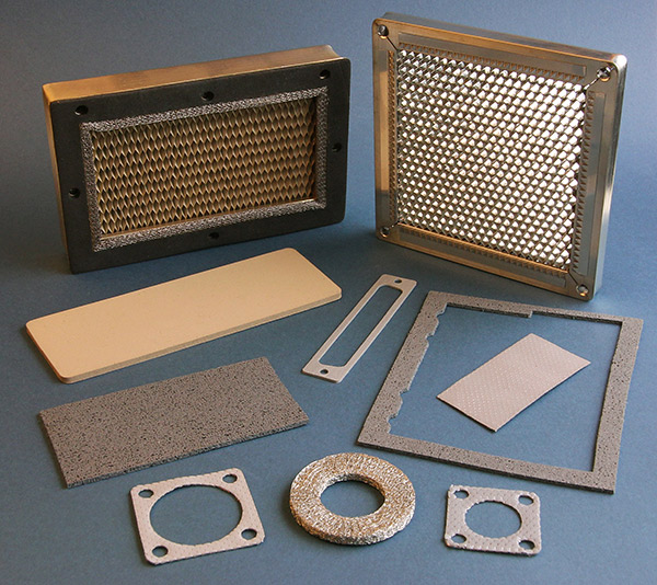
Chemical Etching Technology for EMI/RFI Shielding Covers</h2>In today’s electronics-driven world, where devices operate at ever-higher speeds and frequencies, electromagnetic interference (EMI) and ra
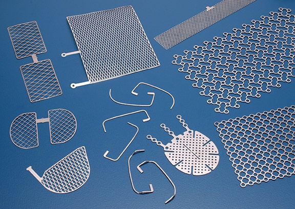
Chemical Etching Technology for Precision Electrodes and Contact Sheets</h2>In high-performance electronic and electrical systems, precision electrodes and contact sheets play a critical role in ensur
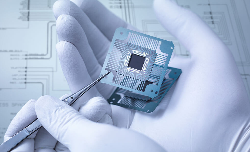
In the semiconductor industry, precision, reliability, and scalability define success. As electronic devices become smaller, faster, and more powerful, the demand for ultra-fine metal components with exacting tolerances continues to grow. Among these components, lead frames play a crucial role — they form the electrical connection between the semiconductor chip and the external circuitry of an integrated circuit (IC) package. To meet modern requirements for miniaturization and high performance, chemical etching has become one of the most advanced and efficient manufacturing methods for producing semiconductor lead frames.
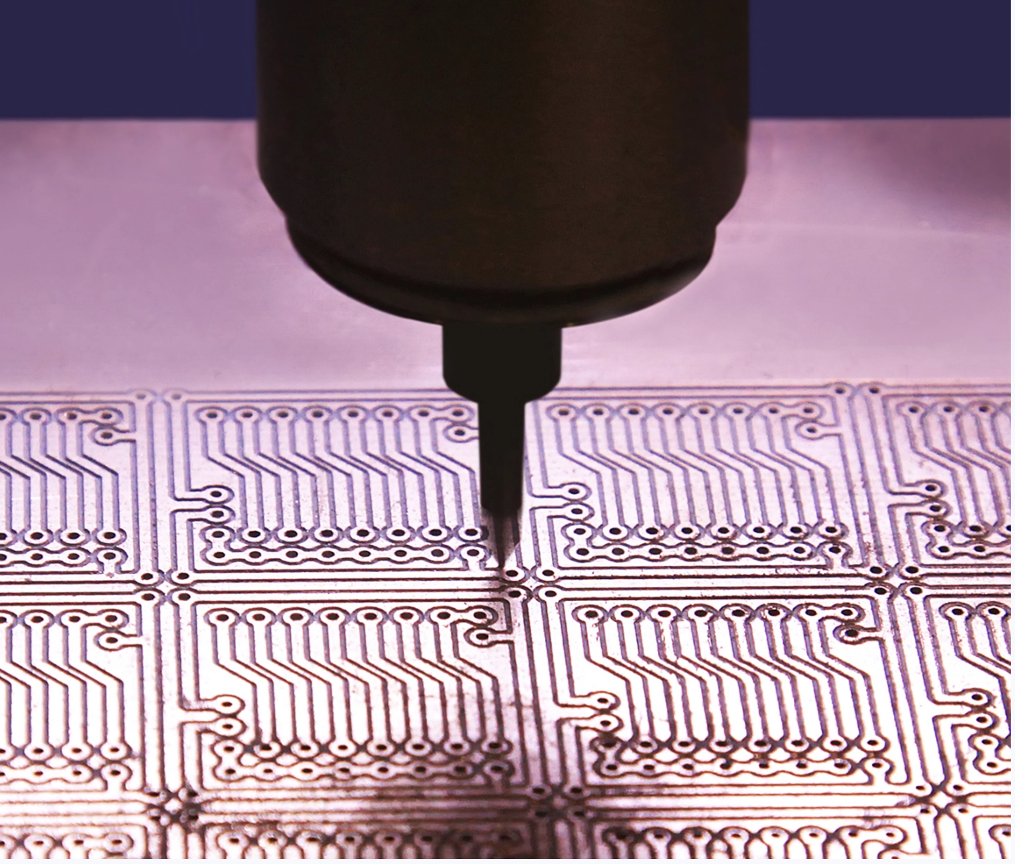
Chemical Etching Technology in PCB Inner Metal Layers As the electronics industry continues to push the boundaries of performance, speed, and miniaturization, the printed circuit board (PCB) has evolved into a sophisticated, multi-layered structure. At the core of every multilayer PCB lie the inner metal layers — the conductive pathways that interconnect signals, distribute power, and ground critical components. Manufacturing these inner layers with precision and consistency is essential for ensuring the reliability and performance of the entire electronic system. Among the various fabrication techniques available, chemical etching has emerged as the most effective and accurate method for creating fine-featured inner metal patterns in modern PCB production.