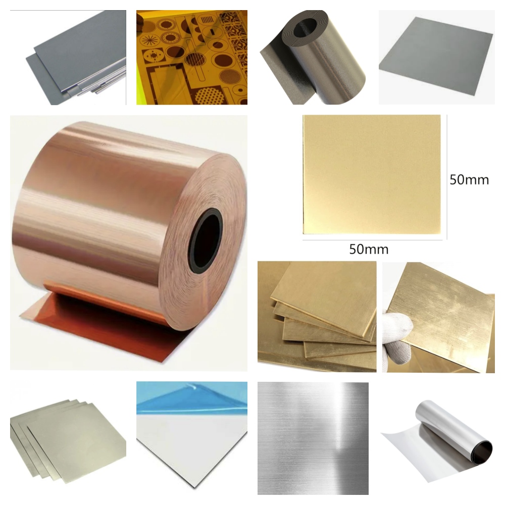
0.2mm minimum trace width PCB Inner Metal Layers
Some information about 0.2mm minimum trace width PCB Inner Metal Layers:
| Type | Chemical Etching&Metal Etching Products |
| Place of Origin | Dongguan,Guangdong |
| Company Name | DRAGON ETCHING |
| Industry experience | 20+years |
| OEM/ODM | Yes |
| Factory Covered | 10000m² |
| Product Size | Customized Size |
| Certificate | ISO9001,CE... |
| Nearby ports | Shenzhen,Guangzhou... |
| Payment | T/T,Visa,DISCOVER,Marst...etc |
| Product Features | Wide range of applications,High quality,Low cost,Broad material compatibility,Flexibility... |
| Warranty | 1 year |
| Material | Metal |
| Transportation | DHL,TNT,FedEx,ARAMEX,EMS...etc |
| Packing Size | 85 * 29 * 90 According to container size, standard export package |
| Terms of delivery | L/C,T/T,Cash... |
| Logo | Customized Logo |
| Color | Red,Grey,White,Yellow, or according to customer requirements |
| Technique | Etching |
| After-sales Service | Online support |
| Trading Country | South america,Africa,North america,Mid east,France,Korea,South Africa,Saudi Arabia,Malaysia,British... |
| Selling Units | Single item |
Please note: The above table data is for reference only. For specific information, please contact us.
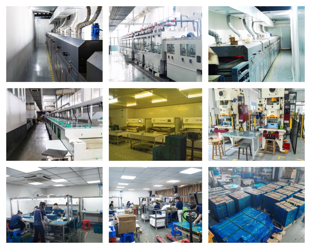
Our Equipment and Workshops
Materials We Can Process for 0.2mm minimum trace width PCB Inner Metal Layers