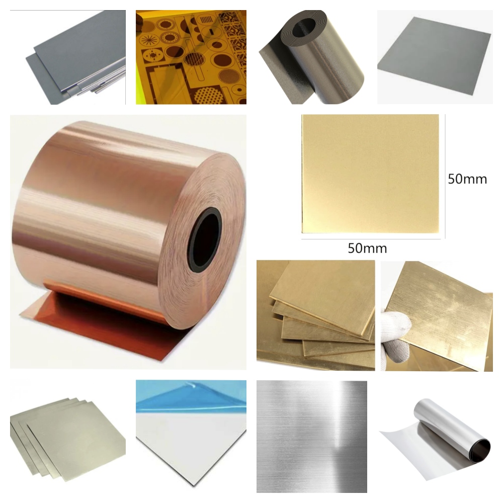
35μm copper weight PCB Inner Metal Layers
Some information about 35μm copper weight PCB Inner Metal Layers:
| Type | Chemical Etching&Metal Etching Products |
| Place of Origin | China |
| Company Name | DRAGON ETCHING TECHNOLOGY., LIMITED |
| Industry experience | 20+years |
| OEM/ODM | Support |
| Factory Covered | 10000m² |
| Product Size | Customized Size |
| Certificate | ISO9001... |
| Nearby ports | Guangzhou,Shenzhen... |
| Payment | Google Play,T/T,Visa,DISCOVER...etc |
| Product Features | High quality,Broad material compatibility,High precision,Low cost... |
| Warranty | 1 year |
| Material | Metal |
| Transportation | DHL,EMS,TNT,ARAMEX,FedEx...etc |
| Packing Size | 98 * 26 * 89 According to container size, standard export package |
| Terms of delivery | L/C,T/T,Cash... |
| Logo | Customized Logo |
| Color | Blue,Yellow,Green, or according to customer requirements |
| Technique | Etching |
| After-sales Service | Online support |
| Trading Country | Africa,Mid east,Europe,South america,Southeast asia,Korea,Malaysia,France,the USA,Italy... |
| Selling Units | Single item |
Please note: The above table data is for reference only. For specific information, please contact us.
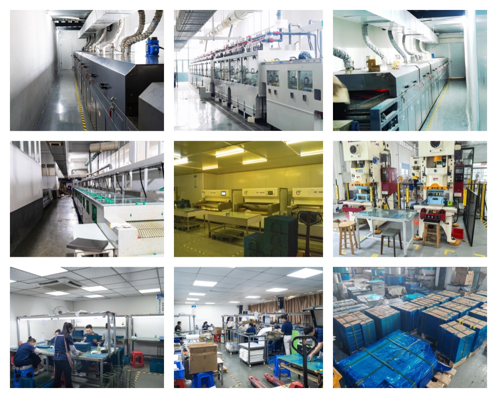
Our Equipment and Workshops
Materials We Can Process for 35μm copper weight PCB Inner Metal Layers